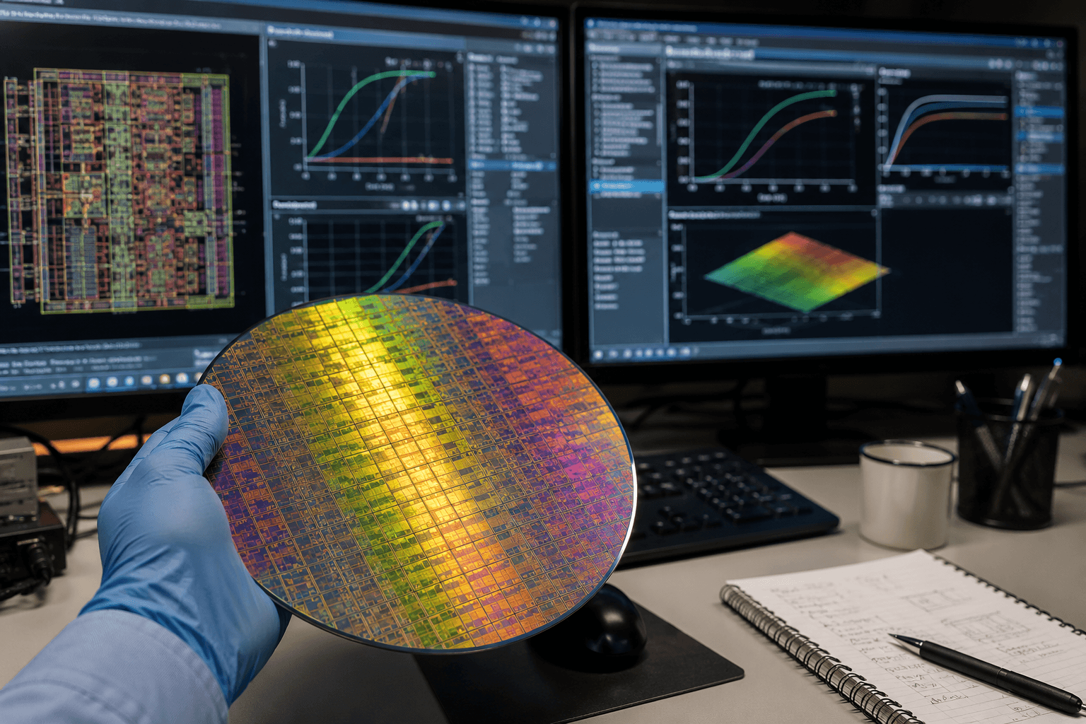
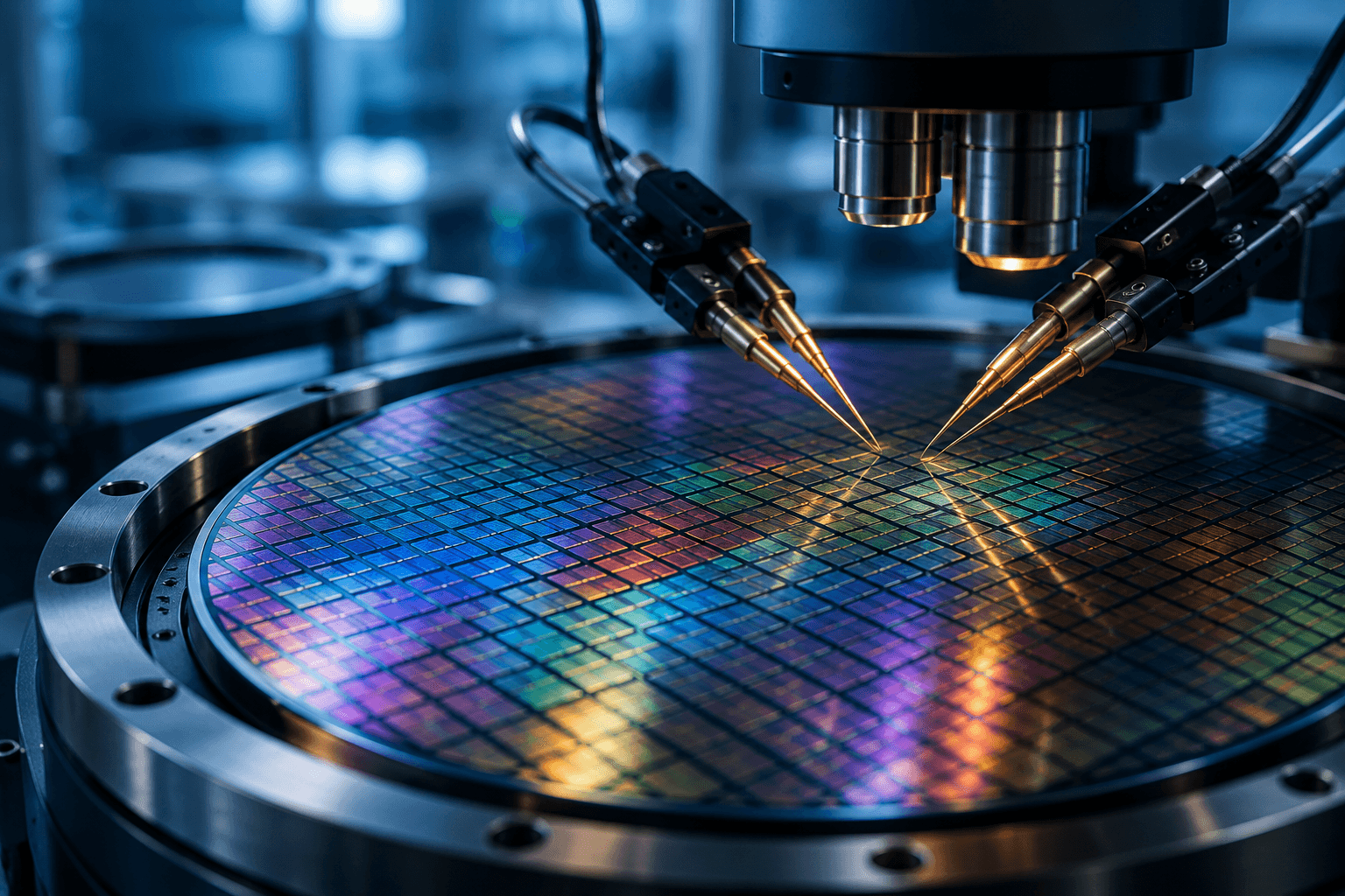
3D-IC Design
Advanced 3D integration, chiplet architecture, die-to-die interfaces, and TSV design for next-gen packaging.
End-to-end IC engineering services from architecture to silicon. Built for innovation. Optimized for performance. Delivered with precision.
CORE SERVICES
Full-stack semiconductor design capability, mapped the way our engineers actually think about a chip.
Advanced 3D integration, chiplet architecture, die-to-die interfaces, and TSV design for next-gen packaging.
Photonic IC design and integration services spanning waveguides, modulators, and electronic-photonic co-packaging for high-bandwidth optical interconnect.
Transceivers, PLLs/synthesizers, and high-speed analog interfaces for 5G, Wi-Fi, automotive, and IoT applications.
Process and device simulation, PDK calibration, and SPICE model extraction using Sentaurus TCAD and Silvaco Atlas/Victory.
Design and engineering support for quantum hardware — from cryo-CMOS control circuitry to qubit interconnect and packaging challenges unique to sub-Kelvin operation.
Full RTL-to-GDSII implementation — synthesis, floorplan, CTS, routing and signoff on nodes down to 3nm.
Expert analog behavioral modeling and AMS verification for faster validation, shorter cycles, and higher design confidence.
UNDER THE FLOORPLAN
The toolchains, nodes, and signoff criteria behind each service area.
ENGAGEMENT MODELS
Flexible delivery structures, built around how chip projects actually run.
RETAINER-BASED
TURNKEY
IP SECURITY
Enterprise-grade protection at our Bangladesh offshore development center.

WHY BOSTON SEMICONDUCTOR
FULL-STACK
From TCAD device physics to physical verification signoff - no handoffs between vendors.
ADVANCED NODE
Tapeouts on TSMC 3nm–28nm, Samsung 5nm, and GlobalFoundries processes.
OUR LOCATIONS
ODC in Bangladesh with headquarters in USA.
IP-SAFE
Biometric ODC access and strict NDAs - your IP never leaves our secure environment.
COMMERCIAL
Retainer or turnkey - we adapt to your project structure and budget.
TRACK RECORD
10+ tapeouts and proven analog IPs, recognized at BEAR 2025.
Blogs
CONTACT us